Introduction
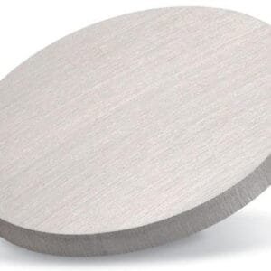
Nickel Antimonide (NiSb) sputtering targets are compound alloy materials used for the deposition of functional intermetallic thin films in semiconductor, thermoelectric, and advanced electronic applications. As a nickel–antimony compound with distinct electrical and structural characteristics, NiSb plays an important role in research related to phase-change materials, topological semimetals, and thermoelectric systems.
Engineered for compositional accuracy and structural stability, NiSb sputtering targets provide a reliable source material for producing stoichiometric thin films with controlled electronic properties.
Detailed Description
Nickel Antimonide is an intermetallic compound formed by combining nickel (Ni) and antimony (Sb) in a defined atomic ratio. Depending on processing conditions, NiSb may crystallize in hexagonal or related structures, influencing its electrical conductivity and magnetic behavior.
High-quality NiSb sputtering targets are manufactured using vacuum melting or powder metallurgy followed by hot pressing or hot isostatic pressing (HIP). These controlled fabrication processes ensure:
Homogeneous elemental distribution
Accurate stoichiometry (near 1:1 atomic ratio)
High density for stable sputtering
Minimal secondary phases
The density and phase uniformity are critical for consistent sputtering rates and film composition control. For high-power magnetron sputtering systems, NiSb targets can be bonded to copper backing plates to enhance thermal conductivity and mechanical strength, reducing the risk of cracking or delamination during long deposition cycles.
NiSb targets are compatible with DC or RF sputtering systems, depending on film design and process parameters.
Applications
Nickel Antimonide sputtering targets are used in:
Thermoelectric Thin Films
NiSb-based materials are investigated for energy harvesting and thermal management systems.Topological and Quantum Materials Research
Used in the study of semimetallic and exotic electronic phases.Semiconductor Device Development
Intermetallic films for contact layers or specialized device structures.Magnetic and Electronic Thin Films
Research on magnetic properties and electronic transport behavior.Advanced Functional Coatings
Tailored thin films for sensors and experimental electronic components.R&D and Academic Research
Widely used in materials science laboratories for compound film deposition.
Technical Parameters
| Parameter | Typical Value / Range | Importance |
|---|---|---|
| Chemical Formula | NiSb | Defines film stoichiometry |
| Purity | 99.9% – 99.99% (3N–4N) | Reduces impurity-induced defects |
| Density | ≥ 95–99% theoretical density | Ensures stable sputtering performance |
| Diameter | 1″ – 6″ (custom available) | Matches sputtering cathodes |
| Thickness | 3 – 10 mm | Affects lifetime and deposition rate |
| Bonding | Cu backing plate optional | Improves heat transfer and stability |
| Fabrication Method | Vacuum melted / HIP processed | Ensures homogeneity and phase control |
Comparison with Related Materials
| Material | Key Advantage | Typical Application |
|---|---|---|
| Nickel Antimonide (NiSb) | Intermetallic stability & unique electronic properties | Thermoelectric & research films |
| Nickel (Ni) | High conductivity & magnetic response | Magnetic films & electrodes |
| Antimony (Sb) | Semimetal behavior | Phase-change & electronic materials |
| Nickel Antimony Alloys (non-stoichiometric) | Tunable properties via composition adjustment | Experimental electronics |
NiSb is selected when precise intermetallic phase behavior and compositional stability are required for functional thin-film development.
FAQ
| Question | Answer |
|---|---|
| Can the Ni:Sb ratio be customized? | Yes, near-stoichiometric or composition-adjusted variants can be supplied upon request. |
| Is bonding recommended for high-power sputtering? | Yes, copper backing plates improve thermal stability during extended runs. |
| Which sputtering method is suitable? | DC sputtering is commonly used; RF is optional depending on system design. |
| Are small R&D quantities available? | Yes, small-diameter targets for laboratory research are supported. |
| How is the product packaged? | Vacuum-sealed with protective foam and export-safe cartons or wooden crates. |
Packaging
Our Nickel Antimonide Sputtering Targets are meticulously tagged and labeled externally to ensure efficient identification and maintain high standards of quality control. We take great care to prevent any potential damage during storage and transportation, ensuring the targets arrive in perfect condition.
Conclusion
Nickel Antimonide (NiSb) sputtering targets offer a dependable solution for depositing intermetallic thin films with controlled electronic and structural properties. Through precise composition control, high-density fabrication, and customizable configurations, NiSb targets support advanced semiconductor research and functional coating development.
For detailed specifications and a quotation, please contact us at sales@thinfilmmaterials.com.


Reviews
There are no reviews yet.