
Silicon Selenium Sputtering Target Description
Silicon Selenide Sputtering Targets offer a range of unique properties that make them particularly valuable for optical and electronic applications. These targets facilitate precise thin-film deposition, ensuring high uniformity and accuracy in the production of optical coatings and electronic devices. As a result, Silicon Selenide Sputtering Targets are extensively used in the fabrication of optical components, optoelectronic devices, and advanced thin-film technologies. Additionally, their strong chemical stability allows them to perform reliably in complex manufacturing environments, making them a dependable material for high-tech industries.
Related Product: Aluminum Silicon Copper Sputtering Target, Aluminum Silicon Sputtering Target
Silicon Selenium Sputtering Target Specifications
| Compound Formula | Si-Se |
| Molecular Weight | 107.045 |
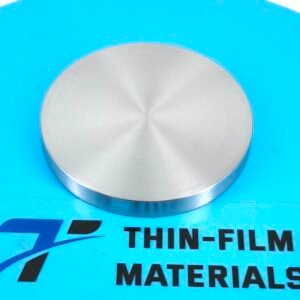
| Appearance | Black Target |
| Available Sizes | Dia.: 1.0″, 2.0″, 3.0″, 4.0″, 5.0″, 6.0″ Thick: 0.125″, 0.250″ |
Silicon Selenium Sputtering Target Handling Notes
Indium bonding is advised for Silicon Selenium Sputtering Targets because certain characteristics of this material make it less suitable for conventional sputtering methods. Due to its brittleness and low thermal conductivity, Silicon Selenium is prone to thermal shock, which can cause issues during the sputtering process. Indium bonding helps to address these challenges by providing a more stable and reliable attachment, ensuring consistent performance and durability of the sputtering targets under operational conditions.
Silicon Selenium Sputtering Target Application
Optical Coating Preparation: Silicon Selenide Sputtering Targets are commonly utilized in the creation of optical coatings, including reflective films, transparent conductive films, and optical filters. The material’s dark gray-to-black color, coupled with its excellent optical properties, makes it a preferred choice for enhancing the performance of optical components.
Optoelectronic Device Manufacturing: These targets are integral in producing optoelectronic devices such as lasers, photodetectors, and optical sensors. The precision offered by Silicon Selenide in thin film deposition is key to achieving the high performance required by these advanced technologies.
Thin Film Technology Applications: In the realm of thin film technology, Silicon Selenide Sputtering Targets are employed to coat electronic devices and other surfaces, thereby enhancing their optical properties and chemical stability, making them more resilient and effective in various applications.
Solar Cells: The unique properties of Si-Se films make them promising candidates for use in solar cells, where they can significantly improve light absorption and enhance the efficiency of electrical energy conversion.
Silicon Selenium Sputtering Target Packaging
Our Silicon Selenium Sputtering Target is carefully handled during storage and transportation to preserve the quality of our products in their original condition.


Reviews
There are no reviews yet.