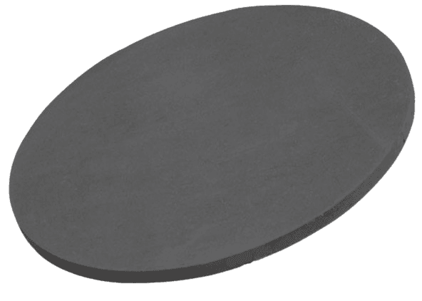
Tantalum Boride Sputtering Target Description
A Tantalum Boride Sputtering Target is a type of boride ceramic material composed of tantalum and boron, used in sputtering processes. This target is typically employed in thin film deposition and various specialized applications, leveraging the unique properties of the tantalum-boron combination.
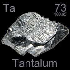 Tantalum is a chemical element named after King Tantalus, a character from Greek mythology and father of Niobe. It was first identified in 1802 by the Swedish chemist Anders Gustaf Ekeberg. The element is represented by the symbol “Ta” and has an atomic number of 73. Tantalum is located in Period 6 and Group 5 of the periodic table, belonging to the d-block elements. Its relative atomic mass is approximately 180.94788 Daltons, with the number in parentheses indicating a margin of uncertainty.
Related Product: Tantalum Sputtering Target
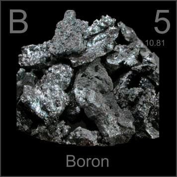 Boron is a chemical element with the symbol “B” and an atomic number of 5. Its name originates from the Arabic word ‘buraq,’ referring to borax. The element was first mentioned in 1808 by Louis-Joseph Gay-Lussac and Louis-Jacques Thénard, with its isolation later achieved and announced by Sir Humphry Davy. Boron is found in Period 2 and Group 13 of the periodic table, classified under the p-block elements. Its relative atomic mass is approximately 10.811 Daltons, with the number in parentheses indicating a margin of uncertainty.
Tantalum Boride Sputtering Target Application
The Tantalum Boride Sputtering Target is utilized in a wide range of applications, including thin film deposition and decorative coatings. It is widely employed in the semiconductor industry, display technologies, and the manufacturing of LEDs and photovoltaic devices. Additionally, this material is essential for functional coatings, the optical information storage industry, glass coating for automotive and architectural purposes, and optical communication technologies.
Tantalum Boride Sputtering Target Packing
Our Tantalum Boride (TaB2) Sputtering Targets are meticulously tagged and labeled on the exterior to ensure efficient identification and maintain stringent quality control. We take extensive precautions to protect these targets from any potential damage during storage and transportation, ensuring they arrive in optimal condition.


Reviews
There are no reviews yet.