1. Introduction: Quantum Materials Meet Thin Film Engineering
Quantum materials—systems whose macroscopic properties arise from quantum mechanical phenomena like electron correlation, topology, and spin entanglement—represent one of the most dynamic frontiers in condensed matter physics.
Traditionally, these effects were studied in bulk single crystals. However, thin film technology has transformed the field by allowing scientists and engineers to manipulate structure, strain, and interfaces with atomic precision.
When grown as thin films, quantum materials exhibit emergent properties such as:
- Tunable electronic band topology
- Enhanced spin–orbit coupling effects
- Quantum coherence at elevated temperatures
- Interfacial superconductivity and magnetism
This shift from bulk to film enables integration into devices—making thin-film quantum materials the practical foundation for the coming generation of quantum electronics, topological transistors, and superconducting qubits.
2. Defining Quantum Materials in the Thin Film Context
The term quantum material covers a broad range of systems whose properties are dominated by quantum effects rather than classical ones.
Key categories relevant to thin-film research include:
- Topological Insulators (TIs):
Materials such as Bi₂Se₃, Bi₂Te₃, and Sb₂Te₃ exhibit insulating bulk behavior but conductive, spin-polarized surface states protected by time-reversal symmetry.
Thin films of TIs allow control over surface–bulk coupling and enable interface engineering for spintronic devices. - Weyl and Dirac Semimetals:
Materials like TaAs and Cd₃As₂ host relativistic quasiparticles with linear dispersion near Weyl or Dirac points.
Thin-film synthesis allows exploration of symmetry-breaking effects and Berry curvature control. - Correlated Electron Systems:
Nickelates, cuprates, and vanadates exhibit Mott transitions and unconventional superconductivity, which are highly sensitive to strain and dimensional confinement. - Two-Dimensional Quantum Materials:
Including graphene, transition metal dichalcogenides (TMDs), and oxide monolayers—exhibiting phenomena like valley polarization and charge density waves. - Unconventional Superconductors:
NbN, YBa₂Cu₃O₇₋ₓ, and FeSe films demonstrate quantum coherence that can be tuned by film thickness, epitaxy, or interfacial effects.
Thin films offer a practical route to quantum functionality by design, bridging fundamental physics with scalable device integration.
3. Thin Film Growth Techniques for Quantum Materials
3.1 Molecular Beam Epitaxy (MBE)
MBE remains the gold standard for atomic-layer control and has enabled groundbreaking discoveries in topological and superconducting thin films.
However, its low throughput limits industrial scalability.
3.2 Pulsed Laser Deposition (PLD)
PLD offers flexibility for complex oxides and superconductors, such as YBCO or nickelates. The ablation of multi-element targets preserves stoichiometry, critical for correlated materials.
3.3 Magnetron Sputtering
Magnetron sputtering—particularly RF and DC sputtering—is increasingly adopted for scalable synthesis of quantum thin films, offering:
- High purity and uniformity over large areas
- Compatibility with industrial deposition systems
- Tunable film composition via alloyed or composite targets
For example, Bi₂Te₃, Sb₂Te₃, and NbN thin films are routinely sputtered using high-density TFM targets with controlled grain structures and dopant levels.
3.4 Atomic Layer Deposition (ALD)
ALD complements sputtering by providing angstrom-level control of ultra-thin barriers or seed layers—essential for interface engineering in hybrid quantum systems.
3.5 Hybrid PVD–ALD Systems
Emerging hybrid systems combine PVD’s deposition speed with ALD’s atomic precision, creating ideal environments for heterostructure quantum films (e.g., TI–superconductor junctions).
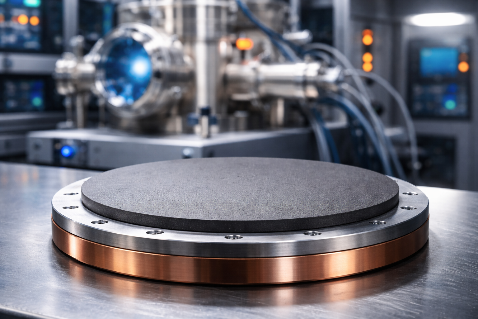
4. Sputtering Targets for Quantum Thin Film Fabrication
The performance of quantum films heavily depends on the quality, purity, and microstructure of the sputtering target.
TFM and other advanced suppliers provide materials tailored for precise stoichiometry and defect control.
| Material System | Function in Quantum Devices | Typical Target Composition |
|---|---|---|
| Bi₂Se₃, Bi₂Te₃ | Topological insulator films | Bi:Se = 2:3 or Bi:Te = 2:3, 99.999% purity |
| Sb₂Te₃, (Bi,Sb)₂Te₃ | Alloyed topological systems | Tunable Sb/Bi ratio for Dirac point control |
| NbN, NbTiN | Superconducting films | High Tc, used in Josephson junctions and qubits |
| VO₂, NdNiO₃ | Correlated oxide films | Exhibiting metal–insulator transition |
| SrTiO₃, LaAlO₃ | Quantum interface templates | Used for 2DEG (two-dimensional electron gas) systems |
| MoTe₂, WTe₂ | Type-II Weyl semimetals | Transition metal chalcogenide targets |
| FeSe, FeTe | Iron-based superconductors | Co-evaporated or co-sputtered multi-element targets |
Advanced targets often employ hot-pressed or HIP sintering to achieve >98% theoretical density, minimizing particulates and ensuring reproducible thin-film composition.
5. Quantum Phenomena Enabled by Thin Films
5.1 Topological Surface States
Thin films allow control over surface coupling and quantum confinement in topological insulators.
When Bi₂Se₃ films are thinner than six quintuple layers, the top and bottom surface states hybridize, opening a tunable energy gap—a crucial step toward topological transistors.
5.2 Two-Dimensional Electron Gas (2DEG) Interfaces
Heterostructures such as LaAlO₃/SrTiO₃ exhibit emergent 2DEG conductivity confined to a few atomic layers.
Strain and interface polarity—controlled via thin-film growth—determine carrier density and mobility.
5.3 Superconductivity and Quantum Coherence
In NbN and YBCO films, film thickness directly influences superconducting critical temperature (Tc).
Ultra-thin NbN films (5–10 nm) enable single-photon detectors and superconducting qubits in quantum information technologies.
5.4 Spin–Orbit Coupling and Spintronics
Topological films with strong spin–orbit coupling, like (Bi,Sb)₂Te₃, exhibit spin-momentum locking, enabling dissipationless spin currents.
Integration with ferromagnetic or superconducting layers creates Majorana modes, a building block for fault-tolerant quantum computing.
5.5 Quantum Phase Transitions
Dimensional confinement in thin films induces phase transitions between metallic, insulating, and superconducting states—enabling quantum phase engineering.
6. Characterization Techniques for Quantum Thin Films
Advanced thin film characterization is crucial for verifying quantum behavior:
- X-Ray Diffraction (XRD): Determines crystallinity and epitaxial alignment.
- X-Ray Photoelectron Spectroscopy (XPS): Verifies stoichiometry and surface oxidation states.
- Angle-Resolved Photoemission Spectroscopy (ARPES): Maps electronic band structures and Dirac cones.
- Scanning Tunneling Microscopy (STM): Visualizes surface states and local density of states.
- Transport Measurements: Reveal quantum oscillations, weak antilocalization, or superconducting transitions.
TFM’s high-purity sputtering targets minimize unintentional doping and impurity scattering—critical for achieving clean quantum transport.
7. Thin Film Integration in Quantum and Spintronic Devices
7.1 Topological Transistors
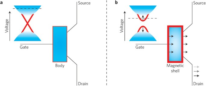
Heterostructures combining TIs with normal insulators or magnetic layers can function as topological field-effect transistors (TFETs), offering low-dissipation switching.
7.2 Josephson Junctions and Superconducting Qubits
Thin-film NbN and NbTiN are indispensable for superconducting quantum circuits due to their:
- High critical temperature (Tc ≈ 15 K)
- Robustness under magnetic fields
- Compatibility with nanolithography
7.3 Quantum Sensors and Detectors
NbN-based superconducting nanowire single-photon detectors (SNSPDs) offer exceptional sensitivity for optical quantum communication.
7.4 Spin–Orbit Torque Devices
Topological films such as Bi₂Se₃ interfaced with ferromagnets (e.g., CoFeB) generate efficient spin currents, enabling energy-efficient memory and logic devices.
7.5 Oxide Electronics
Quantum oxide interfaces (e.g., SrTiO₃-based heterostructures) exhibit tunable superconductivity and ferroelectricity—core components in neuromorphic and quantum devices.
8. Challenges and Future Outlook
Despite tremendous progress, several challenges remain for thin-film quantum materials:
- Defect Control: Even ppm-level impurities can destroy topological protection or superconducting coherence.
- Stoichiometry Uniformity: Maintaining precise element ratios during sputtering is difficult for multi-component chalcogenides.
- Interface Stability: Chemical interdiffusion and lattice mismatch degrade electronic properties.
- Scalability: Transferring MBE-quality films to wafer-scale production remains a bottleneck.
Future directions include:
- AI-Assisted Process Optimization: Machine learning for predictive thin-film growth and defect minimization.
- Hybrid Quantum Architectures: Combining 2D materials, topological insulators, and superconductors.
- Industrial Integration: Scalable magnetron sputtering of quantum films for sensors, spintronics, and quantum processors.
- Reproducible Target Design: Advanced bonding and composite target systems for complex stoichiometries.
9. The Role of Material Suppliers Like TFM
High-performance quantum thin films begin with high-purity, precisely engineered sputtering targets.
TFM contributes by providing:
- Custom Bi–Te, Nb–N, and oxide targets with ≥99.999% purity
- Hot-pressed, defect-free microstructures for uniform sputtering
- Composite or alloyed targets for topological heterostructures
- Technical support for process optimization and film characterization
As thin films continue to shape the future of quantum technology, the partnership between materials innovation and quantum engineering becomes essential.
10. Conclusion
Thin films have emerged as the cornerstone of practical quantum materials research and device development.
Through the precise control of structure, composition, and interface, thin film technology transforms exotic quantum phenomena into scalable, manufacturable components.
From topological insulators to superconductors, each innovation rests on the foundation of advanced material science—where high-purity sputtering targets and deposition expertise define the frontier.
As the field advances, companies like TFM will remain vital partners, enabling the transition from quantum discovery to quantum application—one atomic layer at a time.