A Comprehensive Guide for Materials Scientists, Engineers, and Device Manufacturers
Introduction
In the realm of advanced manufacturing and nano-scale engineering, the integrity of a thin film isn’t measured by thickness alone—it’s also defined by the internal stress it carries. Whether you’re depositing thin films for semiconductors, solar cells, MEMS, optical coatings, or hard protective layers, thin film stress is one of the most critical factors affecting performance, durability, and reliability.
Residual stress—the tension or compression present in a thin film after deposition—can cause warping, delamination, cracking, and changes in electronic or optical behavior. These effects become even more pronounced as film thicknesses shrink below the micron or even nanometer scale.
Understanding what causes stress in thin films—and how to control or minimize it—is essential for any research lab or production facility. This article offers a deep dive into the factors that influence thin film stress, from deposition parameters and material selection to thermal mismatches and crystallographic effects.
What Is Thin Film Stress?

Thin film stress refers to the internal force per unit area present within a film after it’s deposited onto a substrate. It is generally categorized as:
- Tensile stress: Pulls the film outward; can cause cracking or peeling.
- Compressive stress: Pushes the film inward; can lead to wrinkling or buckling.
Stress can be either intrinsic (arising from the film growth process) or extrinsic (due to external factors like temperature changes or substrate bending). In real-world applications, both types often coexist.
Why Does Thin Film Stress Matter?
Unchecked film stress can result in:
- Device failure in microelectronics due to delamination or metal line fracture
- Deformation of optical components, affecting reflectivity or refractive index
- Performance degradation in MEMS due to stiction or mechanical fatigue
- Yield loss in semiconductor fabrication due to substrate warping
Hence, managing thin film stress is not just about achieving dimensional control—it’s about preserving the functionality and stability of the final device.
Core Factors That Influence Thin Film Stress
Let’s explore the main variables that contribute to stress during thin film deposition.
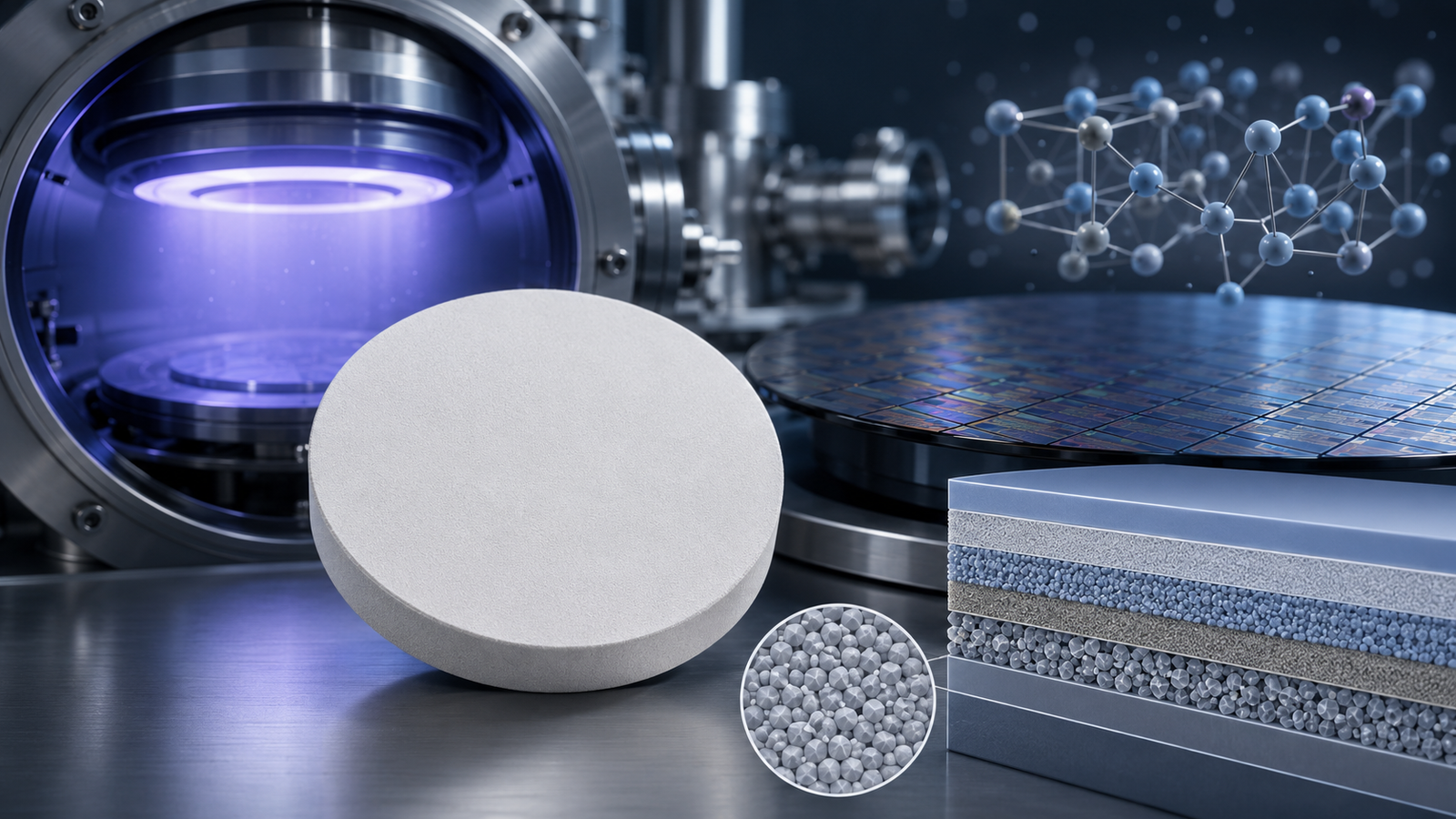
1. Deposition Method
Different thin film deposition techniques inherently produce different stress profiles:
Physical Vapor Deposition (PVD)
- Techniques like sputtering, thermal evaporation, and e-beam evaporation often generate compressive stress due to high-energy particle bombardment.
- Co-sputtering or HiPIMS can lead to denser films with higher stress.
Chemical Vapor Deposition (CVD)
- Low-pressure CVD (LPCVD) tends to yield tensile stress, especially at high temperatures.
- Plasma-enhanced CVD (PECVD) can vary depending on ion energy and film growth conditions.
Atomic Layer Deposition (ALD)
- ALD offers low-stress films due to its self-limiting reactions and uniform growth.
Keyword integration: “low stress ALD coatings”, “PECVD film stress”, “HiPIMS sputtered film properties”
2. Deposition Parameters
Several controllable factors during the deposition process influence residual stress:
a. Deposition Rate
- Higher rates can lead to less dense, porous films—often more tensile.
- Slower rates typically allow for atomic rearrangement, resulting in compressive stress.
b. Substrate Temperature
- Elevated substrate temperatures promote grain growth and stress relaxation.
- Cooling rates post-deposition also impact thermally-induced stress.
c. Working Gas Pressure
- In sputtering, higher argon pressure can lead to lower-energy deposition, promoting columnar microstructures and tensile stress.
- Low pressure results in more energetic particle impact and compressive stress.
d. Target-Substrate Distance
- Alters the energy and directionality of impinging atoms.
3. Material Composition
Material selection influences stress due to differences in:
- Atomic size and bonding structure
- Thermal expansion coefficients
- Crystallographic texture
Examples:
- Metallic films (e.g., Cu, Al) tend to exhibit lower intrinsic stress due to their ductility.
- Ceramic films (e.g., TiO₂, Si₃N₄) are prone to higher stress due to their rigidity.
- Multi-component films (e.g., oxynitrides, silicides) may experience phase separation or volume change.
Keyword integration: “stress in ITO thin films”, “TiN sputtered film cracking”, “multilayer optical film stress”
4. Substrate Effects
The properties of the substrate significantly impact how stress is distributed in the film:
a. Thermal Expansion Mismatch
- When a film and substrate expand or contract at different rates during cooling, thermal stress occurs.
- Common in glass, silicon, or polymer substrates coated with metal or oxide films.
b. Surface Roughness
- Rough substrates can induce localized stress concentration or variable film thickness.
c. Adhesion Quality
- Poor interfacial bonding results in delamination under tensile stress.
d. Substrate Thickness
- Thinner substrates are more likely to deform under stress, affecting film behavior and deposition uniformity.
5. Film Thickness and Multilayer Architecture
Film stress isn’t always constant throughout its depth. Factors include:
- Thin films (<100 nm) may exhibit more tensile stress due to incomplete coalescence of islands.
- Thicker films often relieve stress through grain boundary diffusion or dislocation formation.
- Multilayer coatings can alternate between compressive and tensile layers to balance overall stress.
Example: Hard coatings like TiN/CrN multilayers use this principle for stress compensation.
6. Microstructure and Grain Growth

The microstructure of a thin film—whether amorphous, nanocrystalline, or columnar—dictates how atoms pack and relax:
- Amorphous films (e.g., SiO₂) generally have low stress but poor mechanical strength.
- Columnar structures often contain voids, leading to tensile stress.
- Densely packed grains can generate compressive stress due to atomic peening.
Grain boundaries also act as stress concentrators or relaxation channels, depending on film and temperature.
7. Post-Deposition Treatments
Post-processing steps can dramatically alter film stress:
a. Thermal Annealing
- Relieves intrinsic stress through grain growth and diffusion.
- Must be carefully managed to avoid cracking from sudden phase changes.
b. Ion Implantation or Ion Beam Milling
- Can relieve surface stress or smoothen morphology.
- Used in precision optics and semiconductor tuning.
c. Laser or Plasma Treatments
- Tailor stress profile through localized heating or densification.
Keyword integration: “annealing effect on thin film stress”, “ion beam relaxed coatings”, “laser stress relief in MEMS films”
Methods for Measuring Thin Film Stress
You can’t manage what you don’t measure. Here are common stress measurement techniques:
1. Wafer Curvature (Stoney’s Equation)
- Measures substrate bending before and after film deposition.
- Most widely used in silicon wafer-based processes.
2. X-Ray Diffraction (XRD)
- Analyzes crystallographic strain, offering insight into intrinsic stress.
3. Raman Spectroscopy
- Useful for thin film stress mapping in semiconductors and dielectric layers.
4. Nanoindentation
- Evaluates mechanical stress through localized hardness and elastic modulus.
5. Laser Interferometry
- Precise method for MEMS and micro-optics, detecting nanoscale warping.
Strategies to Minimize or Engineer Thin Film Stress
Here’s how to reduce or optimize stress for better film performance:
- Adjust sputtering pressure and power
- Use substrate heating or biasing
- Introduce multilayers or graded interfaces
- Switch to low-stress deposition techniques like ALD
- Apply annealing cycles to relieve built-in stress
- Opt for stress-compensated materials (e.g., Mo/Cr combinations)
- Utilize rotating or tilted substrates for more uniform atomic arrival angles
Real-World Examples
Semiconductor Interconnects
Copper films deposited on silicon must balance adhesion, low resistance, and minimal stress to prevent cracking during thermal cycling.
Optical Filters
Multi-layer films on glass (e.g., MgF₂/TiO₂) must be stress-balanced to maintain flatness and optical clarity.
Flexible Electronics
Transparent conductors like ITO or ZnO:Al must have low tensile stress to withstand bending without cracking.
Aerospace Coatings
Hard films like DLC or TiAlN must sustain high compressive stress for wear resistance, while avoiding peeling under mechanical load.
Conclusion
Thin film stress is a complex but manageable challenge that intersects physics, chemistry, and materials science. From process engineers tuning sputtering conditions to researchers developing next-generation coatings, understanding the factors that influence stress allows for smarter design, better durability, and higher device reliability.
With a strategic approach—considering deposition method, materials, substrate, and post-processing—thin film stress can be not just minimized but engineered to enhance functionality.
If you’re sourcing sputtering targets or developing custom coatings, a supplier like ThinFilmMaterials.com can provide not just high-purity materials, but also technical insight into how your target choices influence film stress behavior.
Related Products
TFM provides a diverse selection of sputtering targets suitable for various deposition techniques:Thin Film Materials+1Thin Film Materials+1
- Pure Metal Targets: High-purity metals like Indium, Molybdenum, and Iron Boride.
- Alloy Targets: Customizable alloys for specific applications.Maruyasu+8Materion+8Materion+8
- Ceramic Targets: Oxide ceramics like Al₂O₃, SiO₂, and TiO₂.
- Rare Earth Targets: Specialized materials for advanced technologies.Thin Film Materials+5indiumcorporation+5ASM+5
- Rotary Targets: Designed for large-area coating systems.